Photo-Voltaic Panels
|
M.Cricchio,
L.Ferrazzano, A.Vergato (*) - Linguistic Mediator: R.Triggiano (*)
|
|
(*) Istituto Alfano
I
|
Photovoltaic cells.
A solar cell, or photovoltaic cell, is a semiconductor
device that converts photons (light) into electricity. Fundamentally,
the device needs to fulfill only two functions:
- Photogeneration of charger carriers (electrons and holes) in a light-absorbing
material.
- Separation of the charge carriers, preferably to a conductive contact
that will transmit the electricity.
The conversion is called photovoltaic effect: it consists in generation
of electromotive force. The most common configuration of this device,
the first generation photovoltaic, consists of a large-area, single layer
p-n junction diode, which in the presence of sunlight is capable of generating
usable
electrical energy. These cells are typically made using a
silicon p-n junction. However, successive generations of photovoltaic cells that
may improve the photoconversion efficiency are currently being developed.
The second generation of photovoltaic materials is based on multiple layers
of p-n junction diodes. Each layer is designed to absorb a successively
longer
wavelength of light (lower energy), absorbing more of the solar
spectrum and increasing the amount of electrical energy collected. The
third generation of photovoltaics is very different, and is broadly defined
as a semiconductor device which does not rely on a traditional p-n junction
to separate photogenerated charge carriers. They include dye sensitzed
cells, organic polymer cells, and quantum dot solar cells. The absorption
of photons creates electron-hole pairs, which diffuse to the electrical
contacts and can be extracted to power electrical devices. Light generation
of carriers Solar cells have many applications. They are particularly
well suited to, and historically used in, situations where electrical
power from the grid is unavailable, such as in remote area power systems,
Earth orbiting satellites, handheld calculators, remote radiotelephones
and water pumping applications.
When a photon
When a
photon of light hits a piece of silicon, one of two things can
happen. The first is that the photon can pass straight through the silicon
(if the
energy of the photon is lower than the bandgap energy of the silicon
semiconductor). The second thing that can happen is that the photon is
absorbed by the silicon (if the photon energy is greater than the bandgap
energy of silicon). When a photon is absorbed, its energy is given to
an electron in the crystal lattice. Usually this electron is in the
valence band, and is tightly bound in covalent bonds between neighboring atoms,
and hence unable to move far. The energy given to it by the photon "excites"
it into the
conduction band, where it is free to move around within the
semiconductor. The covalent bond that the electron was previously a part
of now has one less electron - this is known as a hole. The presence of
a missing covalent bond allows the bonded electrons of neighboring atoms
to move into the "hole," leaving another hole behind, and in this way
a hole can move through the lattice. Thus, it can be said that photons
absorbed in the semiconductor create mobile electron-hole pairs.A photon
only needs to have energy greater than the band gap energy to excite an
electron from the valence band into the conduction band. However, the
solar
frequency spectrum approximates a
black body spectrum at ~6000 K,
and as such, much of the solar radiation reaching the
Earth is composed
of photons with energies greater than the band gap of silicon. These higher
energy photons will be absorbed by the solar cell, but the difference
in energy between these photons and the silicon band gap is converted
into heat (via lattice vibrations - called
phonons) rather than into usable
electrical energy.
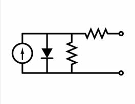 |
Equivalent circuit of a solar cell
To understand the electronic behaviour of a solar cell, it
is useful to create a
model which is electrically equivalent, and
is based on discrete electrical components . An ideal solar cell
may be modelled by a current source in parallel with a diode. In
practice no solar cell is ideal, so a shunt resistance and a series
resistance component are added to the model. The result is the "equivalent
circuit of a solar cell" shown in the picture.
|
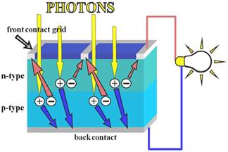
Connection to an external load
Ohmic
metal-semiconductor contacts are made to both the n-type and p-type
sides of the solar cell, and the electrodes connected to an external load.
Electrons that are created on the n-type side, or have been "collected"
by the junction and swept onto the n-type side, may travel through the
wire, power the load, and continue through the wire until they reach the
p-type semiconductor-metal contact. Here, they recombine with a hole that
was either created as an electron-hole pair on the p-type side of the
solar cell, or swept across the junction from the n-type side after being
created there. Usually, solar cells are electrically connected, and combined
into "modules", or
solar panels. Solar panels have a sheet of glass on
the front, and a resin encapsulation behind to keep the semiconductor
wafers safe from the elements (rain, hail, etc). Solar cells are usually
connected in
series in modules, so that their
voltages add.
Silicon as a photovoltaic material
Silicon is a semiconductor as a solid material, meaning that there are
certain
bands of energies which the electrons are allowed to have, and
other energies between these bands which are forbidden. These forbidden
energies are called the "band gap".At room temperature, pure silicon is
a poor electrical conductor. In quantum mechanics, this is explained by
the fact that the Fermi level lies in the forbidden band-gap. To make
silicon a better conductor, it is "doped" with very small amounts of atoms
from either group 13 (III) or group 15 (V) of the periodic table. These
"dopant" atoms take the place of the silicon atoms in the crystal lattice,
and bond with their neighbouring Si atoms in almost the same way as other
Si atoms do. However, because group 13 atoms have only 3 valence electrons,
and group 15 atoms have 5 valence electrons, there is either one too few,
or one too many electrons to satisfy the four covalent bonds around each
atom. Since these extra electrons, or lack of electrons (known as "holes")
are not involved in the covalent bonds of the crystal lattice, they are
free to move around within the solid. Silicon which is doped with group
13 atoms (aluminium, gallium) is known as p-type silicon because the majority
charge carriers (holes) carry a positive charge, whilst silicon doped
with group 15 atoms (phosphorus, arsenic) is known as n-type silicon because
the majority charge carriers (electrons) are negative. It should be noted
that both n-type and p-type silicon are electrically neutral, i.e. they
have the same numbers of positive and negative charges, it is just that
in n-type silicon, some of the negative charges are free to move around,
while the converse is true for p-type silicon.
Semiconductor diodes
In a
p-n junction, conventional current can flow from the p-type side
(the
anode) to the n-type side (the
cathode), but not in the opposite
direction and the current-voltage, or I-V, characteristic curve is ascribed
to the behavior of the so-called
depletion layer or depletion zone which
exists at the
p-n junction between the differing semiconductors. When
a p-n junction is first created, conduction band (mobile) electrons from
the N-doped region diffuse into the P-doped region where there is a large
population of holes (places for electrons in which no electron is present)
with which the electrons "recombine". When a mobile electron recombines
with a hole, the hole vanishes and the electron is no longer mobile. Thus,
two charges carriers have vanished. The region around the p-n junction
becomes depleted of
charge carriers and thus behaves as an
insulator.
However, the
depletion width cannot grow without limit. For each electron-hole
pair that recombines, a positively-charged dopant ion is left behind in
the N-doped region, and a negatively charged dopant ion is left behind
in the P-doped region. As recombination proceeds and more ions are created,
an increasing electric field develops through the depletion zone which
acts to slow and then finally stop recombination. At this point, there
is a 'built-in' potential across the depletion zone. If an external voltage
is placed across the diode with the same polarity as the built-in potential,
the depletion zone continues to act as an insulator preventing a significant
electric current. However, if the polarity of the external voltage opposes
the built-in potential, recombination can once again proceed resulting
in substantial electric current through the p-n junction.
Types of Silicon Solar Cells
Crystalline silicon solar cells come in three primary categories:
- Single crystal or monocrystalline wafers made using the
Czochralski process (or CZ). Most commercial monocrystalline cells have efficiencies
on the order of 1617%. Single-crystal cells tend to be expensive, and
because they are cut from cylindrical ingots, they cannot completely
cover a module without a substantial waste of refined silicon. Additionally
monocrystalline panels have uncovered gaps at the corners of four cells.
- Poly or multi crystalline silicon solar cells are made from cast
ingots - large crucibles of molten silicon carefully cooled and solidified.
These cells are cheaper than single crystal cells and only slightly
less efficient (typically ~1516%). They can also be formed into square
shapes that cover a greater fraction of a panel than monocrystalline
cells.
- Ribbon silicon is formed by drawing flat thin films from molten silicon
having a multicrystalline structure. These cells have even lower efficiencies
(~13.515%), but there is very little silicon waste, as this approach
does not require sawing from ingots.
All three of these technologies are wafer-based manufacturing. In other
words, in each of the above approaches, self-supporting wafers 180-240
micrometres thick are processed into solar cells and then soldered together
to form a module.
- Amorphous silicon films (a-Si) or thin-film silicon solar cells are
fabricated using chemical vapor deposition techniques, typically plasma
enhanced (PE-CVD). These cells have low efficiencies of around 8%, however
they are much less costly to produce.
Amorphous silicon has a higher bandgap (1.7 eV) than crystalline silicon
(c-Si) (1.1 eV), which means it is more efficient to absorb the visible
part of the solar spectrum, but it fails to collect an important part
of the spectrum : the
infrared. As nanocrystalline Si has about the same
bandgap as c-Si, the two material can be combined by depositing two diodes
on top of each other creating a layered cell called a tandem cell. The
top cell in a-Si absorbs the visible light and leaves the infrared part
of the spectrum for the bottom cell in nanocrystalline Si. A patented
silicon thin film technology being developed for building integrated photovoltaics
(BIPV) is semi-transparent solar cells which can be applied as window
glazing. These cells function as window tinting while generating electricity.
Links

http://www.fsec.ucf.edu/pvt/pvbasics/ (make it yourself)
http://www.re-energy.ca/pdf/cp_solarcar.pdf
http://home.earthlink.net/~bdewey/EV_solarpower.html (solar glossary), (solar history timeline)
http://www.eere.energy.gov/solar/photovoltaics.html
Top - Previous
Module - Next Module |